From AI computing clusters to the next generation of data centers, Full Optical Switching (OCS) is becoming the core technology for breaking through the barriers of bandwidth and power consumption. The Semiconductor Optical Amplifier (SOA), a “photonics version of the Swiss knife” that combines amplification, switching, modulation, and detection functions, is undoubtedly the essential “superpowerful heart” of OCS.
1. Why does the AI computing era require OCS? What role does SOA play in this context?
As large-scale model training moves towards use of million-core GPU clusters, traditional electrical switching networks encounter three major problems: each optical signal must go through a conversion between optical and electrical signals before being transmitted further. This results in microseconds of latency, with half of the cluster’s time spent waiting for signals to be transmitted. Additionally, the power consumption associated with switching and interconnection processes accounts for more than 40% of the total electricity costs in data centers. Furthermore, the bandwidth limits of electronic components make it difficult to support 800G/1.6T optical modules.
Optical Circuit Switching (OCS) directly performs signal routing in the optical domain. Signals never undergo conversion to electrical form during transmission, resulting in latency that’s compressed to the nanosecond level. Power consumption is reduced by over 70%, and a single optical fiber can handle speeds of 100 Tbps. The core of OCS switching matrices lies in semiconductor optical amplifiers (SOAs).

Figure: Schematic diagram of the working principle of SOA – Current injection in the active waveguide, resulting in stimulated emission of incident light
SOA essentially refers to a semiconductor laser that eliminates the feedback from the resonant cavity. When a forward current is applied to the active region, population inversion causes the incident light to gain energy (typically 15-30 dB). When the current is shut off, the active region strongly absorbs the light signal, resulting in high isolation levels (>50 dB). This combination of “conductive amplification” and “off-state absorption” capabilities, along with nanosecond-level switching speed, make SOA an ideal switching element for optical switching matrices.
2.Three classic architectures for building OCS exchange matrices using SOA
Depending on the scale of the network, there are three mainstream implementations of OCS based on SOA.
2.1 Broadcasting – Selection Architecture (4×4 to 32×32)

Diagram of the broadcast-selection architecture: signals are transmitted through the splitter, and the output signal is enabled via SOA
Principle: The input signal is broadcast through a 1×N splitter to all output channels. Before each output terminal, there is a SOA configured as a gate switch. When the SOA is activated, the signal is amplified and output; when it is deactivated, the signal is absorbed.
Advantages: No blocking issues, simple structure, and easy control. At a scale of 16×16, the overall switching latency is less than 30ns, with a power consumption of only about 20 watts. The required number of SOAs is N², making it suitable for small-scale edge data centers.
2.2 MZI-SOA hybrid architecture (64×64 to 256×256)

Diagram of the MZI-SOA structure: two 3dB couplers, with both arms integrated as SOAs
Principle: The Mach-Zehnder interferometer (MZI) consists of two arms, each of which contains a SOA component. By adjusting the injection currents of the SOA components in the two arms, the phase difference and amplitude ratio of the light can be controlled, thereby creating interference patterns either in the constructive state or in the destructive state. The extinction ratio can exceed 50 dB.
Advantages: Can be extended in multiple levels up to 1024 ports. The crosstalk interference is extremely low, and the latency is less than 50ns (for 256 ports). It is the mainstream solution for mid-to-large-sized OCS systems.
2.3 Spatial division cross-matrices (very large size, ≥512×512)

Figure: Empty division cross-matrices – N×N cross-point arrays. Each cross-point operates independently under SOA principles
Principle: Each input-output intersection is equipped with an independent SOA. Any input can be connected to any output, and both multicast and broadcast capabilities are supported. Due to the redundant design, any SOA failure can be resolved within 10 nanoseconds by switching to the backup path.
Advantages: It offers the highest level of connectivity flexibility, making it ideal for use in core nodes of backbone networks and supercomputing centers.
3.Beyond just scaling up: Seven “hidden” features of SOA
The characteristics of semiconductor active waveguides make SOA more than just a optical amplifier. By adjusting the direction and magnitude of the bias current, SOA can be transformed into various functional devices.
| Functional mode | Working conditions | Typical applications |
| Broad-spectrum light sources | Lower forward current (ASE mode) | Passive device testing, WDM idle channel filling |
| External cavity laser gain medium | RSOA+ Silicon-based micro-ring external cavity | Narrow-line-width tunable laser (for coherent communication) |
| Full-wave wavelength conversion | Utilizing the non-linear effects of XGM/XPM | Full-optical routing, time-frequency transmission |
| Adjustable amplifier/attenuator | Forward bias (amplification) / Reverse bias (attenuation) | ROADM power balance |
| High-speed optical pulse modulator | Fast on-off current (<1ns) | OTDR, distributed fiber optic sensing |
| Photographic detectors | Reverse bias, measuring photocurrent | On-chip power monitoring for PIC devices |
| Phase modulator | Current alters the refractive index | PSK signal generation, MZI switch phase control |
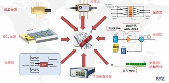
Diagram showing the switching of seven functional modes in SOA architecture – Different working areas under various bias conditions
A single SOA device can replace multiple discrete components such as amplifiers, attenuators, modulators, and detectors. This significantly reduces the size and cost of photonic integration systems.
4. Goptica's SOA Series Products: Domestic, self-developed core optical components
Goptica offers a range of semiconductor optical amplifier products, covering the wavelength range of 1270nm to 1550nm. These products come in various forms, such as bare chips, COCs, and butterfly-packaged devices. They are suitable for applications in optical communication amplification, fiber optic sensing, lidar, and OCS switching matrices. Click to view the complete product list and customization options: SOA Product Overview Page
Typical product 1: 1550nm butterfly package SOA
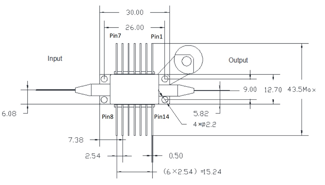
Figure 1550nm Butterfly-shaped SOA component details and pin definitions
| Parameters | Typical values | Notes |
| Operating wavelength | 1480-1590nm 1480–1590nm | Covering the C+L band |
| 3dB Gain Bandwidth | ≥55nm | Wide spectrum applicability
|
| Small signal gain | 25-30dB | @Pin=-25dBm |
| Saturation output power | 12-16dBm 12–16 dBm | 3dB compression point |
| Polarization-related gain | <1dB | Low polarization sensitivity |
Dimming ratio (switching state)
| >50dB | Turn-off isolation level |
| Switch rise/fall time | <1ns <1ns> | Nanosecond-level switching |
| Operating current/voltage | 250-400mA / 1.8V | Constant current drive |
| Total power consumption | <4W | Temperature control with TEC |
| encapsulation | Butterfly shape, COC, bare chip | Optional polarization protection/isolator/PD devices |
This product features a sealed inorganic packaging, integrated TEC thermoelectric cooling and temperature monitoring capabilities. Its operating temperature range is -10 to 70°C, while the storage temperature range is -40 to 85°C. The gas tightness reaches an level of 1×10⁻¹² Pa·m³/s, making it suitable for long-term operation in harsh environments.
Typical product 2: 1270nm SOA chip
| Parameters | Typical values |
| Saturation Light Power | 10dBm |
| Small signal gain | 15-18dB |
| Chip size | 900×400×100μm³ |
| Operating current range | 120-250mA |
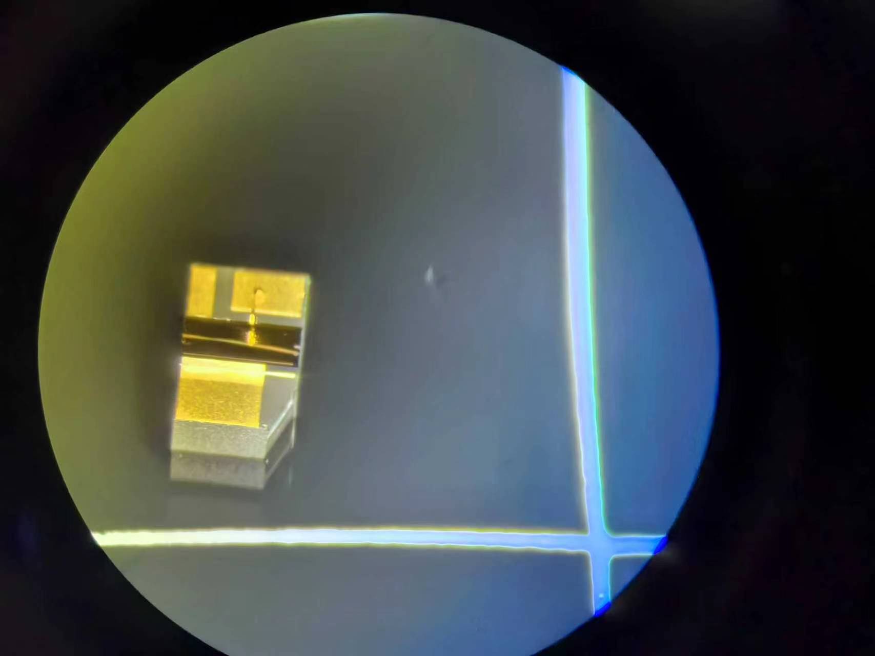
Figure 1270nm SOA chip micrograph – smaller than a sesame seed
This chip is extremely small in size, allowing it to be directly integrated with other on-chip systems such as silicon optical waveguides and detectors. This provides crucial support for high-density photonic integration. Goptica achieves full-process domestic autonomy by using its own chips. Additionally, the chip supports customized configurations such as polarization protection, integrated isolators, and integrated PD optical power monitoring. For more information on various packaging options and customization requirements, please visit the product page for more details.
5. Four major system-level advantages: Why OCS is indispensable without SOAP?
5.1 Nanosecond-level fast scheduling
The MEMS optical switch has a switching time of 1-10 milliseconds due to mechanical movements, while the thermo-optical switch operates over a few microseconds. The SOA mechanism relies entirely on charge carrier injection and extraction, resulting in a switching time of less than 1 nanosecond. The overall switching delay of the 256-port OCS can be controlled within 100 nanoseconds, which is 4-5 orders of magnitude faster than the MEMS solution. For frequent synchronous communications during AI training, nanosecond-level switching significantly reduces synchronization delays, thereby improving the utilization of cluster’s computing resources.
5.2 Built-in gain compensation eliminates cascading losses
The passive optical switch has a insertion loss of 2-3 dB per stage. The total loss of a 16×16 Clos network is 8-12 dB. Due to severe signal attenuation, an external EDFA amplifier is required. The SOA switch provides a gain of 15-30 dB in the on state. It can be designed such that the net gain per stage is greater than 0 dB. The signal power increases across multiple stages, eliminating the need for external amplifiers. This simplifies the system and reduces costs.
5.3 Ultra-low interference and high reliability
The SOA off-state absorption coefficient is extremely high, achieving an isolation level of >50 dB (crosstalk < 10⁻⁵). This ensures that the error rate of 400G signals remains below 10⁻¹². The entire system is solid-state-based, without any mechanical components; thus, the Mean Time Between Fail (MTBF) exceeds 500,000 hours.
5.4 Chip-level integration and low cost
SOA utilizes III-V family semiconductor technologies (such as InP/InGaAsP), and can be integrated or bonded with silicon optical platforms through hetero integration techniques. The 16×16 OCS device has a size comparable to that of a palm, which is only one tenth the size of traditional electrical switching ASICs. Its compatibility with CMOS manufacturing processes means that the cost per port continues to decrease, thereby promoting the adoption of OCSs in both super-large data centers and edge nodes.
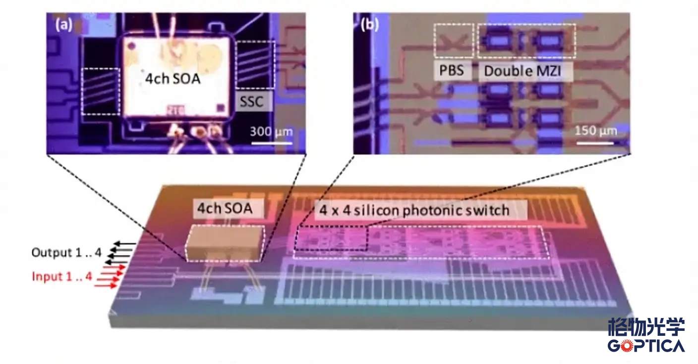
Diagram showing the 4×4 silicon photon switch chip used in SOA integration—a physical device measuring 16×16 micrometers in size, suitable for use in devices the size of a palm
6. Conclusion and Outlook
Since the Ministry of Industry and Information Technology identified optoelectronic chips and OCS devices as the foundation for the development of artificial intelligence, OCS has now been recognized as the core architecture for next-generation data centers at the OFC 2026 conference. Optical switching is indeed entering a golden period of industrialization. According to Cignal AI’s predictions, the market size of OCS will exceed $3 billion by 2029, with a compound growth rate of 58% between 2026 and 2029.
SOA boasts three core capabilities: nanosecond-level switching speed, built-in gain compensation, and chip-level integration. These features make SOA the “ultra-powerful heart” of OCS full-optical switching. In the next three years, SOA+OCS will continue to make breakthroughs in three key areas:
Rate: Evolving from 800G to 1.6T and 3.2T
Scale: From 32×32 to 128×128, 256×256 and even up to thousands of ports.
Integration: Heterogeneous integration of SOA arrays and optical
interconnection chips to build higher-density all-optical
interconnection
Goptica focuses on using autonomous SOA chips as its core technology, specializing in the development of key components for optical amplification and full-optical switching. This enables us to provide robust technical support for the construction of optical networks in the era of AI computing. We welcome you to visit our official website at www.goptica.com, or directly access the SOA product page to view detailed specifications, download data sheets, and submit your customized requirements.